|
|
|
|
|
Next: 6.25 The Transistor |
|
The p-n junction is the work horse of semiconductor applications. This section explains its physical nature, and why it can act as a current rectifier, among other things.
![\begin{figure}\centering
\setlength{\unitlength}{1pt}
\begin{picture}(400,21...
...
\put(200,0){\makebox(0,0)[b]{space charge region}}
\end{picture}
\end{figure}](img1495.gif) |
A p-n junction is created by doping one side of a semiconductor crystal n type and the other side p type. As illustrated at the bottom of figure 6.33, the n side has a appreciable amount of conduction electrons, shown as black dots. These electrons have been provided by donor atoms. The donor atoms, having given up one of their negatively charged electrons, have become positively charged and are shown as encircled plus signs.
The p side has a appreciable number of holes, quantum states that have lost their electrons. The holes are shown as small circles in the figure. Since a negatively charged electron is missing at a hole, the hole behaves as a positively charged particle. The missing electrons have been absorbed by acceptor atoms. These atoms have therefore acquired a negative charge and are shown by encircled minus signs.
The atoms are stuck in the crystal and cannot move. Electrical conduction takes place by means of motion of the electrons and holes. But under normal conditions, significant electrical conduction can only occur in one direction. That makes the p-n junction into a “diode,” a current rectifier.
To see the basic reason is not difficult. In the so-called
forward
direction that allows a significant current,
both the electrons in the n side and the holes in the p
side flow towards the junction between the n and p
sides. (Note that since electrons are negatively charged, they move
in the direction opposite to the current.) In the vicinity of the
junction, the incoming n-side electrons can drop into the
incoming p-side holes. Phrased more formally, the electrons
recombine with the holes. That can readily happen. A forward current
flows freely if a suitable forward-biased
voltage is
applied.
However, if a reverse-biased
voltage is applied, then
normally very little current will flow. For a significant current in
the reverse direction, both the electrons in the n side and the
holes in the p side would have to flow away from the junction.
So new conduction electrons and holes would have to be created near
the junction to replace them. But random thermal motion can create
only a few. Therefore there is negligible current.
While this simple argument explains why a p-n junction can act as a diode, it is not sufficient. It does not explain the true response of the current to a voltage. It also does not explain other applications of p-n junctions, such as transistors, voltage stabilizers, light-emitting diodes, solar cells, etcetera.
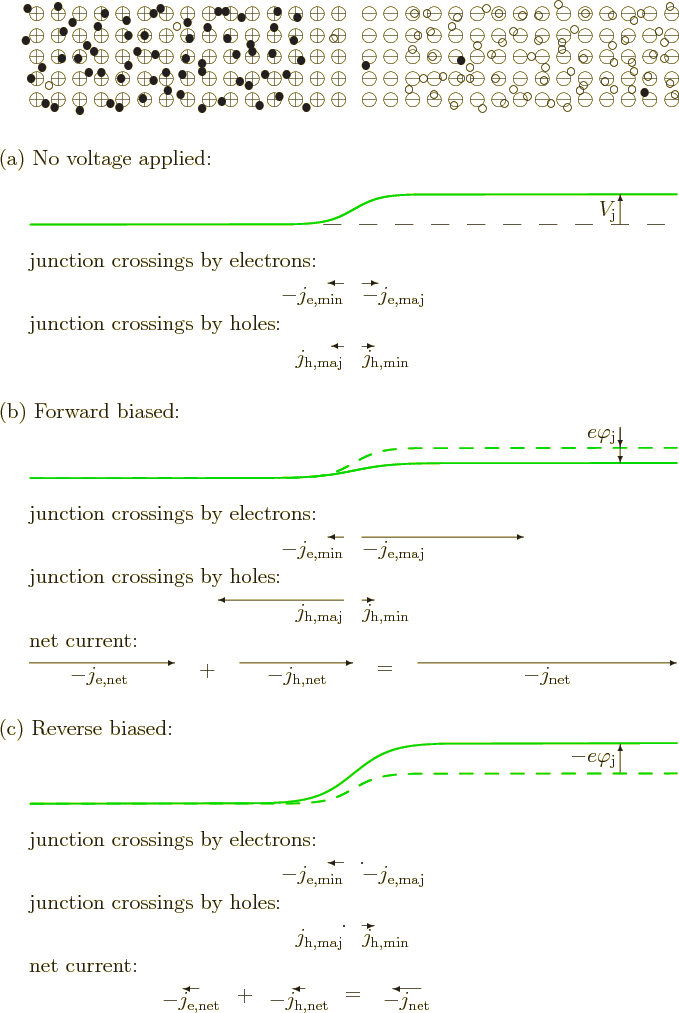
It turns out that in the forward direction, the recombination of the incoming electrons and holes is severely hindered by an electrostatic barrier that develops at the contact surface between the n-type and p-type material. This barrier is known as the “built-in potential.” It is shown in green in figure 6.33.
Consider first the p-n junction in thermal equilibrium, when there is no current. The junction is shown in the lower part of figure 6.33. The n side has an excess amount of conduction electrons. The negative charge of these electrons is balanced by the positively charged donor atoms. Similarly, the p side has an excess amount of holes. The positive charge of these holes is balanced by the negatively charged acceptor atoms.
At the junction, due to random thermal motion the n-side electrons would want to diffuse into the p side. Similarly the p-side holes would want to diffuse into the n side. But that cannot go on indefinitely. These diffusion processes cause a net negative charge to flow out of the n side and a net positive charge out of the p side. That produces the electrostatic barrier; it repels further n-side electrons from the p side and p-side holes from the n side.
The barrier takes the physical form of a double layer of positive charges next to negative charges. This layer is called the “space charge region.” It is illustrated in figure 6.33. Double layers are common at contact surfaces between different solids. However, the one at the p-n junction is somewhat unusual as it consists of ionized donor and acceptor atoms. There are preciously few electrons and holes in the space charge region, and therefore the charges of the donors and acceptors are no longer offset by the electrons, respectively holes.
The reason for the lack of electrons and holes in the space charge region may be understood from figure 6.32: when the numbers of electrons and holes become comparable, there are not many of either. The lack of electrons and holes explains why the space charge region is also known as the “depletion layer.”
The double layer is relatively thick. It has to be, to compensate for
the fact that the fraction of atoms that are donors or acceptors is
quite small. A typical thickness is 1![]()
An n-side electron that tries to make it through the space charge region is strongly pulled back by the positive donors behind it and pushed back by the negative acceptors in front of it. Therefore there is a step-up in the electrostatic potential energy of an electron going through the region. This increase in potential energy is shown in green in figure 6.33. It raises the electron energy levels in the p side relative to the n side. In particular, it makes the chemical potentials, or Fermi levels, of the two sides equal. It has to do so; differences in chemical potential produce net electron diffusion, section 6.16. For the diffusion to stop, the chemical potential must become everywhere the same.
There is still some flow of electrons and holes through the junction, even in the absence of net current. It is due to random thermal motion. To simplify its description, it will be assumed that there is no significant recombination of electrons and holes while they pass through the space charge region, nor creation of new electrons and holes. That is a standard assumption, but by no means trivial. It requires great purification of the semiconductor. Crystal defects can act as “recombination centers,” locations that help the electrons and holes recombine. For example, if you try to simply press separate n and p crystals together to create a p-n junction, it will not work. It will have far too many defects where the crystals meet. A proper recombination of electrons and holes should take place near the junction, but mostly outside the space charge region.
Consider now first the thermal flow of electrons and holes through the
junction when there is no net current. It is sketched in figure
6.34a. All those n-side electrons would love
to diffuse into the p side, but the electrostatic barrier is
holding them back. Only very few electrons have enough energy to make
it through. The required amount of energy is the electrostatic energy
increase over the junction. That energy will be called
![]() .
.![]()
![]()
The crossings of these few very lucky electrons produce a miniscule
current through the junction. It is indicated as ![]()
![]()
![]() .
.
The miniscule current of the n-side majority electrons is
balanced by an equally miniscule but opposite current ![]()
For holes the story is equivalent. Because they have the opposite charge from the electrons, the same barrier that keeps the n-side electrons out of the p side also keeps the p-side holes out of the n side.
The bottom line is that there is no net current. And there should not be; otherwise you would have a battery that worked for free. Batteries must be powered by a chemical reaction.
But now suppose that a forward-bias
external voltage
![]()
![]() .
.![]() .
.![]()
The currents of minority carriers do not change appreciably. Whatever minority carriers diffuse into the space charge region still all pass through it. Note that the Fermi levels of the n and p sides do no longer match up when there is a current. If there is a current, the system is not in thermal equilibrium.
Figure 6.34c shows the case that a reverse bias voltage is applied. The reverse voltage increases the barrier for the majority carriers. The number that still have enough energy to cross the junction gets decimated to essentially zero. All that remains is a residual small reverse current of minority carriers through the junction.
Based on this discussion, it is straightforward to write a ballpark
expression for the net current through the junction:
For forward bias the exponential explodes, producing significant current. For reverse bias, the exponential is essentially zero and only the small reverse minority current is left.
Equation (6.37) is known as the “Shockley diode equation.” It works well for germanium but not quite that well for silicon. Silicon has a much larger band gap. That makes the minority currents much smaller still, which is good. But the correspondingly small reversed-biased and slightly forward-biased currents are sensitive to depletion layer electron-hole generation, respectively recombination. A fudge factor called the “ideality factor” is often added to the argument of the exponential to improve agreement.
Even for germanium, the Shockley diode equation applies only over a
limited range. The equation does not include the resistance of the
semiconductor. If the current increases rapidly, the voltage drop due
to resistance does too, and it should be added to the voltage drop
![]()
Key Points
- The p-n junction is the interface between an n-type and a p-type side of a semiconductor crystal.
- Under normal conditions, it will only conduct a significant current in one direction, called the forward direction.
- In the forward direction both the n-side electrons and the p-side holes move towards the junction.
- The Shockley diode equation describes the current versus voltage relation of p-n junctions, but only in a limited range.
- At the junction a space-charge region exists. It provides a barrier for the majority carriers. However, it accelerates the minority carriers passing through the junction.