|
|
|
|
|
Next: 6.24 The P-N Junction |
|
Semiconductors are at the core of modern technology. This section
discusses some basic properties of semiconductors that will be needed
to explain how the various semiconductor applications work. The main
semiconductor manipulation that must be described in this section is
doping,
adding a small amount of impurity atoms.
 |
If semiconductors did not conduct electricity, they would not be very
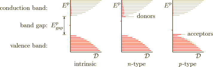
useful. Consider first the pure, or “intrinsic,” semiconductor. The vicinity of the band gap in its
spectrum is shown to the left in figure 6.31. The vertical
coordinate shows the energy ![]()
![]() ,
,
Time for a reality check. The number of such electrons and holes is
very much smaller than the figure indicates. The number
![]()
For an intrinsic semiconductor, the Fermi level is about in the middle
of the band gap. Therefore the average number of electrons per
quantum state at the bottom of the conduction band is
So it is not surprising that pure silicon conducts electricity poorly.
It has a resistivity of several thousand ohm-m where good metals have
on the order of 1![]() .
.![]()
![]()
And the number of conduction electrons becomes much smaller still at cryogenic temperatures. If the temperature is a frigid 150 K instead of a 300 K room temperature, the number of electrons per state in silicon drops by another factor of a billion. That illustrates one important rule:
You cannot just forget about temperature to understand semiconductors.Usually, you like to analyze the ground state at absolute zero temperature of your system, because it is easier. But that simply does not work for semiconductors.
The number of holes per state in the valence band may be written in a
form similar to that for the electrons in the conduction band:
From a comparison of the expressions for the number of particles per
state ![]()
![]()
![]()
![]()
![]()
Note that figure 6.31 is misleading in the sense that it
depicts the same density of states ![]()
![]()
![]()
![]()
![]()
That illustrates another important rule of thumb for semiconductors:
Keep your eyes on the thermal exponentials. Usually, their variations dwarf everything else.If
(For gallium arsenide, the difference between the densities of states for holes and electrons is much larger than for silicon or germanium. That makes the shift in Fermi level at room temperature more substantial.)
The Fermi level may be directly computed. Expressions for the total
number of conduction electrons per unit volume and the total number of
holes per unit volume are, {D.30}:
The first exponential in (6.35) is the value of the number
of electrons per state ![]()
![]()
That can be greatly improved by what is called doping the material. Suppose you have a semiconductor like germanium, that has 4 valence electrons per atom. If you replace a germanium atom in the crystal by a stray atom of a different element that has 5 valence electrons, then that additional electron is mismatched in the crystal structure. It can easily become dislocated and start roving through the conduction band. That allows additional conduction to occur. Even at very small concentrations, such impurity atoms can make a big difference. For example, you can increase the conductivity of germanium by a factor of a thousand by replacing 1 in a million germanium atoms by an arsenic one.
Because such valence-5 impurity atoms add electrons to the conduction band, they are called “donors.” Because electrical conduction occurs by the negatively charged additional electrons provided by the doping, the doped semiconductor is called “n-type.”
Alternatively, you can replace germanium atoms by impurity atoms that have only 3 valence electrons. That creates holes that can accept valence band electrons with a bit of thermal energy. Therefore such impurity atoms are called “acceptors.” The holes in the valence band from which the electrons were taken allow electrical conduction to occur. Because the holes act like positively charged particles, the doped semiconductor is called “p-type.”
Silicon has 4 valence band electrons just like germanium. It can be doped similarly.
Now consider an n-type semiconductor in more detail. As the center of figure 6.31 indicates, the effect of the donor atoms is to add a spike of energy states just below the conduction band. At absolute zero temperature, these states are filled with electrons and the conduction band is empty. And at absolute zero, the Fermi level is always in between filled and empty states. So the Fermi level is now in the narrow gap between the spike and the conduction band. It illustrates that the Fermi level of a semiconductor can jump around wildly at absolute zero.
But what happens at absolute zero is irrelevant to a room temperature semiconductor anyway. At room temperature the Fermi level is typically as shown by the tick mark in figure 6.31. The Fermi level has moved up a lot compared to the intrinsic semiconductor, but it still stays well below the donor states.
If the Fermi level would still be in the middle of the band gap like for the undoped material, then there would be very few electrons in the donor states. But all the electrons that are in the donor states at absolute zero temperature cannot just disappear into nothing. And they cannot go into the intrinsic states. If the Fermi level does not change, the intrinsic states still have the same number of electrons as before the doping.
So the Fermi level cannot be in the middle of the band gap. And the Fermi level going down makes the missing electron problem worse; then there are even less electrons in the donor states and conduction band, and even more holes in the valence band.
The Fermi level must go up, significantly. For one, that will reduce
the number of holes in the valence band. However, since the number of
such holes is so tiny compared to the nuber of donor electrons, that
does not help much. Much more importantly, the Fermi level ![]()
Do note that while the Fermi level must go up, it cannot move too
close to the donor states either. For assume the contrary, that the
Fermi level is really close to the donor states. Then the donor
states will be largely filled with electrons. But at room temperature
the gap between the donor states and the conduction band is comparable
to ![]() .
.![]()
If more donors are added, the Fermi level will move up more. Light
doping may be on the order of 1 impurity atom in a 100 million, heavy
doping 1 in 10,000. If the donor atoms get too close together, their
electrons start to interact. If that happens the spike of donor
states broadens into a band extending to the conduction band, and you
end up with a metallic “degenerate” semiconductor. For example, low temperature
measurements show that phosphor donors turn silicon metallic at about
1 phosphor atom per 15 000 silicon ones. It may seem strange that
impurity electrons at such a small concentration could interact at
all. But note that 1 impurity in 15 000 atoms means that each
![]()
The p-type material is analyzed pretty much the same as n-type, with holes taking the place of electrons and acceptors the place of donors.
As already mentioned, the upward shift in the Fermi level in the n-type material has another effect besides providing lots of electrons in the conduction band. It decimates the already miserably small number of holes in the valence band that the undoped semiconductor had. That means that virtually all electrical conduction will now be performed by electrons, not holes. The electrons in n-type material are therefore called the “majority carriers” and the holes the “minority carriers.”
 |
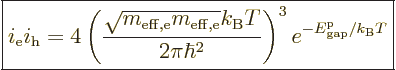
The fact that raising the amount of conduction band electrons lowers
the amount of valence band holes may be verified mathematically from
(6.35). That equation implies that the product of the
electron and hole densities is constant at a given temperature:
electron-hole density relation.And if you come to think of it, what is wrong with the name? Doesn’t pretty much everything in physics come down to masses performing actions? That includes semiconductors too!
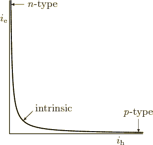
The relationship is plotted in figure 6.32. It shows that a high number of conduction electrons implies a very low number of holes. Similarly a p-type material with a high number of holes will have very few conduction electrons.
The law of mass action can also be understood from more classical
arguments. That is useful since band theory has its limits. The
classical picture is as follows: In thermal equilibrium, the
semiconductor is bathed in blackbody radiation. A very small but
nonzero fraction of the photons of this radiation have energies above
the band gap. These will move valence band electrons to the
conduction band, thus creating electron-hole pairs. In equilibrium,
this creation of electron-hole pairs must be balanced by the removal
of an identical amount of electron-hole pairs. The removal of a pair
occurs through “recombination,” in which an conduction band electron drops back
into a valence band hole, eliminating both. The rate of
recombinations will be proportional to the product of the densities of
electrons and holes. Indeed, for a given number of holes, the more
electrons there are, the more will be able to find holes under
suitable conditions for recombination. And vice-versa with electrons
and holes swapped. Equating a creation rate of electron-hole pairs by
photons, call it ![]() ,
,![]()
![]()
![]()
![]()
![]() .
.![]()
This classical picture also provides an intuitive explanation why
adding both donors and acceptors to a semiconductor does not double
the amount of current carriers over just one type of doping alone.
Quite the opposite. As figure 6.32 shows, if the number of
holes becomes comparable to the number of electrons, there are not
many of either one. The semiconductor behaves again like an intrinsic
one. The reason is that adding, say, some acceptors to an
n-type material has the primary effect of making it much easier
for the conduction band electrons to find valence band holes to
recombine with. It is said that the added acceptors
compensate
for the donors.
Key Points
- Doping a semiconductor with donor atoms greatly increases the number of electrons in the conduction band. It produces an n-type semiconductor.
- Doping a semiconductor with acceptor atoms greatly increases the number of holes in the valence band. It produces an p-type semiconductor.
- The minority carrier gets decimated.
- The Fermi level is in the band gap, and towards the side of the majority carrier.
- There is compensation in doping. In particular, if there are about the same numbers of electrons and holes, then there are not many of either.