|
|
|
|
|
Next: 6.23 Semiconductors |
|
A meaningful discussion of semiconductors requires some background on how electrons move through solids. The free-electron gas model simply assumes that the electrons move through an empty periodic box. But of course, to describe a real solid the box should really be filled with the countless atoms around which the conduction electrons move.
This subsection will explain how the motion of electrons gets modified by the atoms. To keep things simple, it will still be assumed that there is no direct interaction between the electrons. It will also be assumed that the solid is crystalline, which means that the atoms are arranged in a periodic pattern. The atomic period should be assumed to be many orders of magnitude shorter than the size of the periodic box. There must be many atoms in each direction in the box.
 |
The effect of the crystal is to introduce a periodic potential energy for the electrons. For example, figure 6.21 gives a sketch of the potential energy seen by an electron along a line of nuclei. Whenever the electron is right on top of a nucleus, its potential energy plunges. Close enough to a nucleus, a very strong attractive Coulomb potential is seen. Of course, on a line that does not pass exactly through nuclei, the potential will not plunge that low.
![\begin{figure}\centering
\setlength{\unitlength}{1pt}
\begin{picture}(380,53...
...-1,0){184}}
\put(0,-10){\makebox(0,0)[b]{$\ell_x$}}
\end{picture}
\end{figure}](img1441.gif) |
Kronig & Penney developed a very simple one-dimensional model that
explains much of the motion of electrons through crystals. It assumes
that the potential energy seen by the electrons is periodic on some
atomic-scale period ![]() .
.![]()
![]() ,
,crystal.
In particular, the box should contain a large
and whole number of atomic periods.
Three-dimensional Kronig & Penney quantum states can be formed as products of one-dimensional ones, compare chapter 3.5.8. However, such states are limited to potentials that are sums of one-dimensional ones. In any case, this section will restrict itself mostly to the one-dimensional case.
This subsection examines the single-particle quantum states, or energy eigenfunctions, of electrons in one-dimensional solids.
For free electrons, the energy eigenfunctions were given in section
6.18. In one dimension they are:
To find the equivalent one-dimensional energy eigenfunctions
![]()
![]()
However, it can be shown that the eigenfunctions can always be written
in the form:
Energy eigenfunctions of the form (6.32) are called “Bloch waves.” It may be pointed out that this form of the energy eigenfunctions was discovered by Floquet, not Bloch. However, Floquet was a mathematician. In naming the solutions after Bloch instead of Floquet, physicists celebrate the physicist who could do it too, just half a century later.
The reason why the energy eigenfunctions take this form, and what it
means for the electron motion are discussed further in chapter
7.10.5. There are only two key points of interest for
now. First, the possible values of the wave number ![]()
![]()
![]()
![]()
![]() .
.![]()
![]()
![]()
![]()
![]()
![]()
![]()
![]() ,
,
Key Points
- In the presence of a periodic crystal potential, the energy eigenfunctions pick up an additional factor that has the atomic period.
- The wave number values do not change.
- The velocity is found by differentiating the energy with respect to the crystal momentum.
As the previous section discussed, the difference between metals and insulators is due to differences in their energy spectra. The one-dimensional Kronig & Penney model can provide some insight into it.
Finding the energy eigenvalues is not difficult on a computer, {N.9}. A couple of example spectra are shown in figure 6.23. The vertical coordinate is the single-electron energy, as usual. The horizontal coordinate is the electron velocity. (So the free electron example is the one-dimensional version of the spectrum in figure 6.18, but the axes are much more compressed here.) Quantum states occupied by electrons are again in red.
The example to the left in figure 6.23 tries to roughly
model a metal like lithium. The depth of the potential drops in
figure 6.22 was chosen so that for lone
atoms,
(i.e. for widely spaced potential drops), there
is one bound spatial state and a second marginally bound state. You
might think of the bound state as holding lithium’s two inner
1s
electrons, and the marginally bound state as
holding its loosely bound single 2s
valence electron.
Note that the 1s state is just a red dot in the lower part of the
left spectrum in figure 6.23. The energy of the inner
electrons is not visibly affected by the neighboring
atoms.
Also, the velocity does not budge from zero;
electrons in the inner states would hardly move even if there
were unfilled states. These two observations are related, because as
mentioned earlier, the velocity is the derivative of the energy with
respect to the crystal momentum. If the energy does not vary, the
velocity is zero.
The second energy level has broadened into a half-filled
conduction band.
Like for the free-electron gas in
figure 6.18, it requires little energy to move some
Fermi-level electrons in this band from negative to positive
velocities to achieve net electrical conduction.
The spectrum in the middle of figure 6.23 tries to
roughly model an insulator like diamond. (The one-dimensional model
is too simple to model an alkaline metal with two valence electrons
like beryllium. The spectra of these metals involve different energy
bands that merge together, and merging bands do not occur in the
one-dimensional model.) The voltage drops have been increased a bit
to make the second energy level for lone atoms
more
solidly bound. And it has been assumed that there are now four
electrons per atom,
so that the second band is
completely filled.
Now the only way to achieve net electrical conduction is to move some
electrons from the filled valence band
to the empty
conduction band
above it. That requires much more
energy than a normal applied voltage could provide. So the crystal is
an insulator.
The reasons why the spectra look as shown in figure 6.23 are not obvious. Note {N.9} explains by example what happens to the free-electron gas energy eigenfunctions when there is a crystal potential. A much shorter explanation that hits the nail squarely on the head is “That is just the way the Schrödinger equation is.”
Key Points
- A periodic crystal potential produces energy bands.
The spectrum to the right in figure 6.23 shows the
one-dimensional free-electron gas. The relationship between velocity
and energy is given by the classical expression for the kinetic energy
in the ![]() -
-
It is interesting to compare this spectrum to that of the
metal
to the left in figure 6.23. The
occupied part of the conduction band of the metal is approximately
parabolic just like the free-electron gas spectrum. To a fair
approximation, in the occupied part of the conduction band
This illustrates that conduction band electrons in metals behave much like free electrons. And the similarity to free electrons becomes even stronger if you define the zero level of energy to be at the bottom of the conduction band and replace the true electron mass by an effective mass. For the metal shown in figure 6.23, the effective mass is 61% of the true electron mass. That makes the parabola somewhat flatter than for the free-electron gas. For electrons that reach the conduction band of the insulator in figure 6.23, the effective mass is only 18% of the true mass.
In previous sections, the valence electrons in metals were repeatedly approximated as free electrons to derive such properties as degeneracy pressure and thermionic emission. The justification was given that the forces on the valence electrons tend to come from all directions and average out. But as the example above now shows, that approximation can be improved upon by replacing the true electron mass by an effective mass. For the valence electrons in copper, the appropriate effective mass is about one and a half times the true electron mass, [42, p. 257]. So the use of the true electron mass in the examples was not dramatically wrong.
And the agreement between conduction band electrons and free electrons is even deeper than the similarity of the spectra indicates. You can also use the density of states for the free-electron gas, as given in section 6.3, if you substitute in the effective mass.
To see why, assume that the relationship between the energy ![]()
![]()
![]()
![]()
![]()
![]() .
.![]()
![]()
![]()
![]()
It should however be pointed out that in three dimensions, things get messier. Often the effective masses are different in different crystal directions. In that case you need to define some suitable average to use the free-electron gas density of states. In addition, for typical semiconductors the energy structure of the holes at the top of the valence band is highly complex.
Key Points
- The electrons in a conduction band and the holes in a valence band are often modeled as free particles.
- The errors can be reduced by giving them an effective mass that is different from the true electron mass.
- The density of states of the free-electron gas can also be used.
The crystal momentum of electrons in a solid is not the same as the linear momentum of free electrons. However, it is similarly important. It is related to optical properties such as the difference between direct and indirect gap semiconductors. Because of this importance, spectra are usually plotted against the crystal momentum, rather than against the electron velocity. The Kronig & Penney model provides a simple example to explain some of the ideas.
Figure 6.24 shows the single-electron energy plotted
against the crystal momentum. Note that this is equivalent to a plot
against the wave number ![]() ;
;![]()
![]()
![]() .
.![]() .
.
There is however an ambiguity in the figure:
The crystal wave number, and so the crystal momentum, is not unique.Consider once more the general form of a Bloch wave,
Therefore there is a problem with how to define a unique value of
![]() .
.
A second approach is much more common, though. It uses the
indeterminacy in ![]()
![]()
![]()
![]()
![]()
![]()
![]() .
.
But it is much more than that. For one, the different energy curves
in the reduced zone scheme can be thought of as modified atomic energy
levels of lone atoms. The corresponding Bloch waves can be thought of
as modified atomic states, modulated by a relatively slowly varying
exponential ![]() .
.
Second, the reduced zone scheme is important for optical applications of semiconductors. In particular,
A lone photon can only produce an electron transition along the same vertical line in the reduced zone spectrum.The reason is that crystal momentum must be conserved. That is much like linear momentum must be preserved for electrons in free space. Since a photon has negligible crystal momentum, the crystal momentum of the electron cannot change. That means it must stay on the same vertical line in the reduced zone scheme.
To see why that is important, suppose that you want to use a semiconductor to create light. To achieve that, you need to somehow excite electrons from the valence band to the conduction band. How to do that will be discussed in section 6.27.7. The question here is what happens next. The excited electrons will eventually drop back into the valence band. If all is well, they will emit the energy they lose in doing so as a photon. Then the semiconductor will emit light.
It turns out that the excited electrons are mostly in the lowest energy states in the conduction band. For various reasons. that tends to be true despite the absence of thermal equilibrium. They are created there or evolve to it. Also, the holes that the excited electrons leave behind in the valence band are mostly at the highest energy levels in that band.
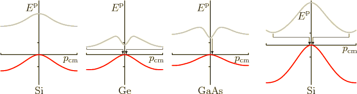
Now consider the energy bands of some actual semiconductors shown to the left in figure 6.26. In particular, consider the spectrum of gallium arsenide. The excited electrons are at the lowest point of the conduction band. That is at zero crystal momentum. The holes are at the highest point in the valence band, which is also at zero crystal momentum. Therefore, the excited electrons can drop vertically down into the holes. The crystal momentum does not change, it stays zero. There is no problem. In fact, the first patent for a light emitting diode was for a gallium arsenide one, in 1961. The energy of the emitted photons is given by the band gap of gallium arsenide, somewhat less than 1.5 eV. That is slightly below the visible range, in the near infrared. It is suitable for remote controls and other nonvisible applications.
But now consider germanium in figure 6.26. The highest point of the valence band is still at zero crystal momentum. But the lowest point of the conduction band is now at maximum crystal momentum in the reduced zone scheme. When the excited electrons drop back into the holes, their crystal momentum changes. Since crystal momentum is conserved, something else must account for the difference. And the photon does not have any crystal momentum to speak of. It is a phonon of crystal vibration that must carry off the difference in crystal momentum. Or supply the difference, if there are enough pre-existing thermal phonons. The required involvement of a phonon in addition to the photon makes the entire process much more cumbersome. Therefore the energy of the electron is much more likely to be released through some alternate mechanism that produces heat instead of light.
The situation for silicon is like that for germanium. However, the lowest energy in the conduction band occurs for a different direction of the crystal momentum. The spectrum for that direction of the crystal momentum is shown to the right in figure 6.26. It still requires a change in crystal momentum.
At the time of writing, there is a lot of interest in improving the light emission of silicon. The reason is its prevalence in semiconductor applications. If silicon itself can be made to emit light efficiently, there is no need for the complications of involving different materials to do it. One trick is to minimize processes that allow electrons to drop back into the valence band without emitting photons. Another is to use surface modification techniques that promote absorption of photons in solar cell applications. The underlying idea is that at least in thermal equilibrium, the best absorbers of electromagnetic radiation are also the best emitters, section 6.8.
Gallium arsenide is called a “direct-gap semiconductor” because the electrons can fall straight down into the holes. Silicon and germanium are called “indirect-gap semiconductors” because the electrons must change crystal momentum. Note that these terms are accurate and understandable, a rarity in physics.
Conservation of crystal momentum does not just affect the emission of light. It also affects its absorption. Indirect-gap semiconductors do not absorb photons very well if the photons have little more energy than the band gap. They absorb photons with enough energy to induce vertical electron transitions a lot better.
It may be noted that conservation of crystal momentum is often called
“conservation of wave vector.” It is the same thing of course,
since the crystal momentum is simply ![]()
(If you wonder why crystal momentum is preserved, and how it even can
be if the crystal momentum is not unique, the answer is in the
discussion of conservation laws in chapter 7.3 and its
note. It is not really momentum that is conserved, but the product of
the single-particle eigenvalues ![]()
![]() .
.![]()
![]()
![]() ,
,![]()
![]()
![]()
Returning to the possible ways to plot spectra, the so-called “periodic zone scheme” takes the reduced zone scheme and extends it periodically, as in figure 6.27. That makes for very esthetic pictures, especially in three dimensions.
Of course, in three dimensions there is no reason for the spectra in
the ![]()
![]()
![]() -
-![]() ,
,![]()
![]()
Similarly, typical spectra for real solids have to show the spectrum versus wave number for more than one crystal direction to be comprehensive. One example was for silicon in figure 6.26. A more complete description of the one-dimensional spectra of real semiconductors is given in the next subsection.
Key Points
- The wave number and crystal momentum values are not unique.
- The extended, reduced, and periodic zone schemes make different choices for which values to use.
- The reduced zone scheme limits the wave numbers to the first Brillouin zone.
- For a photon to change the crystal momentum of an electron in the reduced zone scheme requires the involvement of a phonon.
- That makes indirect gap semiconductors like silicon and germanium undesirable for some optical applications.
A complete description of the theory of three-dimensional crystals is beyond the scope of the current discussion. Chapter 10 provides a first introduction. However, because of the importance of semiconductors such as silicon, germanium, and gallium arsenide, it may be a good idea to explain a few ideas already.
![\begin{figure}\centering
\setlength{\unitlength}{1pt}
\begin{picture}(400,21...
...,0)[bl]{Ga}}
\put(-119,41){\makebox(0,0)[r]{As}}
}
\end{picture}
\end{figure}](img1468.gif) |
Consider first a gallium arsenide crystal. Gallium arsenide has the same crystal structure as zinc sulfide, in the form known as zinc blende or sphalerite. The crystal is sketched in figure 6.28. The larger spheres represent the nuclei and inner electrons of the gallium atoms. The smaller spheres represent the nuclei and inner electrons of the arsenic atoms. Because arsenic has a more positively charged nucleus, it holds its electrons more tightly. The figure exaggerates the effect to keep the atoms visually apart.
The grey gas between these atom cores represents the valence electrons. Each gallium atom contributes 3 valence electrons and each arsenic atom contributes 5. That makes an average of 4 valence electrons per atom.
As the figure shows, each gallium atom core is surrounded by 4 arsenic
ones and vice-versa. The grey sticks indicate the directions of the
covalent bonds between these atom cores. You can think of these bonds
as somewhat polar s![]()
It is customary to think of crystals as being build up out of simple building blocks called “unit cells.” The conventional unit cells for the zinc blende crystal are the little cubes outlined by the thicker red lines in figure 6.28. Note in particular that you can find gallium atoms at each corner of these little cubes, as well as in the center of each face of them. That makes zinc blende an example of what is called a “face-centered cubic” lattice. For obvious reasons, everybody abbreviates that to FCC.
You can think of the unit cells as subdivided further into 8 half-size cubes, as indicated by the thinner red lines. There is an arsenic atom in the center of every other of these smaller cubes.
The simple one-dimensional Kronig & Penney model assumed that the crystal
was periodic with a period ![]() .
.![]() ,
,![]() ,
,![]() .
.
For example, if you start at the center of a gallium atom, you will
again be at the center of a gallium atom. And you can step to
whatever gallium atom you like in this way. At least as long as the
whole multiples are allowed to be both positive and negative. In
particular, suppose you start at the gallium atom with the Ga label in
figure 6.28. Then ![]()
![]()
![]()
The choice of primitive translation vectors is not unique. In
particular, many sources prefer to draw the vector ![]()
![]() ,
,![]() ,
,![]()
You can use the primitive translation vectors also to mentally create the zinc blende crystal. Consider the pair of atoms with the Ga and As labels in figure 6.28. Suppose that you put a copy of this pair at every point that you can reach by stepping around with the primitive translation vectors. Then you get the complete zinc blende crystal. The pair of atoms is therefore called a “basis” of the zinc blende crystal.
This also illustrates another point. The choice of unit cell for a given crystal structure is not unique. In particular, the parallelepiped with the primitive translation vectors as sides can be used as an alternative unit cell. Such a unit cell has the smallest possible volume, and is called a primitive cell.
The crystal structure of silicon and germanium, as well as diamond, is identical to the zinc blende structure, but all atoms are of the same type. This crystal structure is appropriately called the diamond structure. The basis is still a two-atom pair, even if the two atoms are now the same. Interestingly enough, it is not possible to create the diamond crystal by distributing copies of a single atom. Not as long as you step around with only three primitive translation vectors.
For the one-dimensional Kronig & Penney model, there was only a single
wave number ![]()
![]()
![]() ,
,![]() ,
,![]() .
.
In the Kronig & Penney model, the wave numbers could be reduced to a
finite interval
In three dimensions, the first Brillouin zone is no longer a
one-dimensional interval but a three-dimensional volume. And the
separations over which wave number vectors are equivalent are no
longer so simple. Instead of simply taking an inverse of the period
![]() ,
,![]()
![]()
![]() ,
,![]() ,
,![]() ,
,![]() .
.
The shape of the first Brillouin zone is important for understanding graphs of three-dimensional spectra. Every single point in the first Brillouin zone corresponds to multiple Bloch waves, each with its own energy. To plot all those energies is not possible; it would require a four-dimensional plot. Instead, what is done is plot the energies along representative lines. Such plots will here be indicated as one-dimensional energy bands. Note however that they are one-dimensional bands of true three-dimensional crystals. They are not just Kronig & Penney model bands.
Typical points between which one-dimensional bands are drawn are
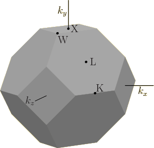
indicated in figure 6.29. You and I would probably name
such points something like F (face), E (edge), and C (corner), with a
clarifying subscript as needed. However, physicists come up with
names like K, L, W, and X, and declare them standard. The center of
the Brillouin zone is the origin, where the wave number vector is
zero. Normal people would therefore indicate it as O or 0. However,
physicists are not normal people. They indicate the origin by
![]()
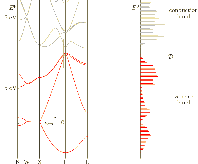 |
Computed one-dimensional energy bands between the various points in the Brillouin zone can be found in the plot to the left in figure 6.30. The plot is for germanium. The zero level of energy was chosen as the top of the valence band. The various features of the plot agree well with other experimental and computational data.
The earlier spectrum for germanium in figure 6.26 showed only the part within the little frame in figure 6.30. That part is for the line between zero wave number and the point L in figure 6.29. Unlike figure 6.30, the earlier spectrum figure 6.26 showed both negative and positive wave numbers, as its left and right halves. On the other hand, the earlier spectrum showed only the highest one-dimensional valence band and the lowest one-dimensional conduction band. It was sufficient to show the top of the valence band and the bottom of the conduction band, but little else. As figure 6.30 shows, there are actually four different types of Bloch waves in the valence band. The energy range of each of the four is within the range of the combined valence band.
The complete valence band, as well as the lower part of the conduction
band, is sketched in the spectrum to the right in figure
6.30. It shows the energy plotted against the density of
states ![]() .
.
An interesting feature of figure 6.30 is that two different
energy bands merge at the top of the valence band. These two bands
have the same energy at the top of the valence band, but very
different curvature. And according to the earlier subsection
6.22.3, that means that they have different effective mass.
Physicists therefore speak of light holes
and
heavy holes
to keep the two types of quantum states
apart. Typically even the heavy holes have effective masses less than
the true electron mass, [29, pp. 214-216]. Diamond is an
exception.
The spectrum of silicon is not that different from germanium.
However, the bottom of the conduction band is now on the line from the
origin ![]()
Key Points
- Silicon and germanium have the same crystal structure as diamond. Gallium arsenide has a generalized version, called the zinc blende structure.
- The spectra of true three-dimensional crystals are considerably more complex than those of the one-dimensional Kronig & Penney model.
- In three dimensions, the period turns into three primitive translation vectors.
- The first Brillouin zone becomes three-dimensional.
- There are light holes and heavy holes at the top of the valence band of typical semiconductors.
![\begin{figure}\centering
\setlength{\unitlength}{1pt}
\begin{picture}(405,20...
...tor}}
\put(135,0){\makebox(0,0)[b]{free electrons}}
\end{picture}
\end{figure}](img1455.gif)
![\begin{figure}\centering
\setlength{\unitlength}{1pt}
\begin{picture}(400,20...
...tor}}
\put(100,0){\makebox(0,0)[b]{free electrons}}
\end{picture}
\end{figure}](img1460.gif)
![\begin{figure}\centering
\setlength{\unitlength}{1pt}
\begin{picture}(400,20...
...tor}}
\put(100,0){\makebox(0,0)[b]{free electrons}}
\end{picture}
\end{figure}](img1463.gif)
![\begin{figure}\centering
\setlength{\unitlength}{1pt}
\begin{picture}(300,20...
...{\rm p}_x$}}
\put(0,0){\makebox(0,0)[b]{insulator}}
\end{picture}
\end{figure}](img1467.gif)