|
|
|
|
|
Next: 6.28 Thermoelectric Applications |
|
|
|
|
|
|
Next: 6.28 Thermoelectric Applications |
|
This section gives a concise overview of optical physics ranging from the x-ray spectrum of solids to semiconductor devices such as solar cells and light-emitting diodes.
Lone atoms have discrete electron energy levels, figure 6.19. An electron can transition from one of these levels to another by emitting or absorbing a photon of light. The energy of the photon is given by the difference in energy between the levels. Therefore emitted and absorbed photons have very specific energies, and corresponding very specific frequencies and wave lengths.
If they are in the visible range, they have very specific colors. The visible range of light corresponds to photons with energies from about 1.6 eV (red) to 3.2 eV (violet). In terms of the wave length of the light, the range is from about 390 nm (violet) to 760 nm (red).
A basic example is the red photon emitted in an ![]()
![]()
Lone atoms can also absorb photons from light that passes them by.
The same wave lengths that they can emit, they can also absorb.
Absorbing a photon puts the atoms in an excited state of higher
energy. They may then subsequently emit a photon identical to the
absorbed one in a different direction. Or they may lose their
excitation energy in a transition between different energy levels,
producing a photon of a different wave length. Or they may lose the
energy in collisions. Either one eliminates the original photon
altogether. For example, an excited hydrogen atom in the ![]()
![]()
![]()
In 1817 Fraunhofer gave a list of dark lines in the spectrum of
sunlight. His list included the red ![]()
![]()
![]()
![]()
A typical solar spectrum also includes absorption lines due to molecules like oxygen and water vapor in the atmosphere of the earth. Molecular spectra tend to be more complicated than atomic ones, especially in the infrared region. That is due to relative motion of the different nuclei. The spectra are also more complicated due to the larger number of electrons involved.
Key Points
- Lone atoms and molecules emit and absorb light at specific wave lengths.
- It allows atoms and molecules to be recognized in the lab or far out in space.
Solids have electron energy levels arranged into continuous bands,
figure 6.19. Therefore solids do not emit discrete wave
lengths of light like lone atoms do. When light from solids is sent
through a prism, the light will spread out into bands of gradually
changing color. That is called broadband
radiation.
To be sure, transitions involving the inner atomic electrons in solids still produce radiation at discrete wave lengths. The reason is that the energies of the inner electrons are not significantly different from the discrete values of the corresponding lone atoms. But because these energies are so much larger in magnitude, the produced radiation is in the X-ray range, not in the visible light range.
Key Points
- Solids can emit and absorb electromagnetic radiation in continuous bands.
- The X-ray range of the inner electrons is still discrete.
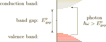
As noted above, the light from solids is not limited to discrete wave lengths like that of lone atoms. But it is not true that solids can emit and absorb all wave lengths. In particular, a perfect crystal of an insulator with a large-enough band gap will be transparent to visible light. Take diamond as an example. Its valence band is completely filled with electrons but its conduction band is empty, as sketched in figure 6.36. A photon of light with enough energy can use its energy to take take an electron out of the valence band and put it into the conduction band. That leaves a hole behind in the valence band and eliminates the photon. However, to do this requires that the photon has at least the band gap energy of diamond, which is 5.5 eV. The photons of visible light have energies from about 1.6 eV to 3.2 eV. That is not enough. Visible light simply does not have enough energy to be absorbed by diamond electrons. Therefore a perfect diamond is transparent. Visible light passes through it unabsorbed.
 |
By this reasoning, all perfect crystals will be transparent if their band gap exceeds 3.2 eV. But actually, the energy of the photon can be somewhat less than the band gap and it may still be able to excite electrons. The model of energy states for noninteracting electrons that underlies spectra such as figure 6.36 is not perfect. The band gap in a spectrum is really the energy to create a conduction band electron and a valence band hole that do not interact. But the electron is negatively charged, and the hole acts as a positive particle. The two attract each other and can therefore form a bound state called an “exciton.” The energy of the photon needed to create an exciton is less than the band gap by the binding energy of the exciton. There is some additional slack due to variations in this binding energy. In the simplest model, the energy levels of lone excitons would be discrete like those of the hydrogen atom. However, they broaden considerably in the less than ideal environment of the solid.
If visible-light photons do not have enough energy to form electron-hole pairs nor excitons, the perfect crystal will be transparent. If the blue side of the visible spectrum has enough energy to excite electrons, the crystal will be colored reddish, since those components of light will remain unabsorbed.
Key Points
- A perfect crystal of a solid with a large enough band gap will be transparent.
- An exciton is a bound state of an electron and a hole.
It should be pointed out that in real life, the colors of most nonmetals are caused by crystal imperfections. For example, in ionic materials there may be a vacancy where a negative ion is missing. Since the vacancy has a net positive charge, an electron can be trapped inside it. That is called an “F-center.” Because its energy levels are relatively small, such a center can absorb light in the visible range. Besides vacancies, chemical impurities are another common cause of optical absorption. A complete description of all the different types of crystal imperfections and their effects is beyond the scope of this book.
Key Points
- The colors of most nonmetals are caused by crystal imperfections.
- An electron bound to a vacancy in a ionic crystal is a called an F-center.
For a nonmetal with a sufficiently narrow band gap, photons of light may have enough energy to take electrons to the conduction band. Then both the electrons in the conduction band, as well as the holes that they leave behind in the valence band, can participate in electrical conduction through the solid. Increased electrical conductivity due to light is called “photoconductivity.” It is used for a variety of light sensing devices and for Xerox copiers.
Note that excitons cannot directly produce electrical conduction, as the complete exciton is electrically neutral. However, excitons can create charge carriers by interacting with crystal imperfections. Or photons with energies less than the band gap can do so themselves. In general, the mechanisms underlying photoconductivity are highly complex and strongly affected by crystal imperfections.
Key Points
- Photoconductivity is the increase in conductivity of nonmetals when photons of light create additional charge carriers.
In the vicinity of a p-n junction in a semiconductor crystal, light can do much more than just increase conductivity. It can create electricity. That is the principle of the “photovoltaic cell.” These cells are also known as solar cells if the source of light is sunlight.
To understand how they work, consider the schematic of a p-n junction in figure 6.33. Suppose that the crystal is exposed to light. If the photons of light have more energy than the band gap, they can knock electrons out of the valence band. For example, silicon has a band gap of about 1.12 eV. And as noted above, the photons of visible light have energies from about 1.6 eV to 3.2 eV. So a typical photon of sunlight has plenty of energy to knock a silicon electron out of the valence band.
That produces a conduction band electron and a valence band hole. The two will move around randomly due to thermal motion. If they are close enough to the junction, they will eventually stumble into its space charge region, figure 6.33. The electric field in this region will forcefully sweep electrons to the n side and holes to the p side. Therefore, if the p-n junction is exposed to a continuous stream of light, there will be a continuous flow of new electrons to the n side and new holes to the p side. This creates a usable electric voltage difference between the two sides: the excess n-side electrons are willing to pass through an external load to recombine with the p-side holes.
There are limitations for the efficiency of the creation of electricity. The excess energy that the absorbed photons have above the band gap ends up as heat instead of as electrical power. And photons with insufficient energy to create electron-hole pairs do not contribute. Having p-n junctions with different band gaps absorb different wave lengths of the incoming light can significantly improve efficiency.
Key Points
- Photovoltaics is the creation of electricity by photons. Solar cells are an important example.
In the photovoltaic effect, light creates electricity. But the opposite is also possible. A current across a p-n junction can create light. That is the principle of the “light-emitting diode” (LED) and the “semiconductor laser.”
Consider again the schematic of a p-n junction in figure 6.33. When a forward voltage is applied across the junction, n-side electrons stream into the p side. These electrons will eventually recombine with the prevailing holes in the p side. Simply put, the conduction electrons drop into the valence band holes. Similarly, p-side holes stream into the n side and eventually recombine with the prevailing electrons at that side. Each recombination releases a net amount of energy that is at least equal to the band gap energy. In a suitably chosen semiconductor, the energy can come out as light.
As section 6.22.4 discussed, silicon or germanium are not
really suitable. They are what is called “indirect band
gap” semiconductors. For these the energy is much more likely
to come out as heat rather than light. Using various tricks, silicon
can be made to emit some light, but the efficiency is low. LEDs
normally use direct band gap
semiconductors. The
classical direct gap material is gallium arsenide, which produced the
first patented infrared LED. To emit visible light, the band gap
should exceed about 1.6 eV. Indeed, as noted earlier, the photons of
visible light range from about 1.6 eV (red) to 3.2 eV (violet). That
relates the band gap of the LED to its color. (For indirect gap
semiconductors a phonon is involved, section 6.22.4, but its
energy is small.) Gallium arsenide, with its 1.4 eV direct band gap
emits infrared light with an average wave length of 940 nm. A 1.4 eV
photon has a wave length of 885 nm. Diamond, with its 5.5 eV indirect
band gap emits some ultraviolet light with an average wave length of
235 nm. A 5.5 eV photon has a wave length of 225 nm.
By the addition of a suitable optical cavity, a “diode laser” can be constructed that emits coherent light. The
cavity lets the photons bounce a few times around through the region
with the conduction electrons and holes. Now it is one of the
peculiar symmetries of quantum mechanics that photons are not just
good in taking electrons out of the valence band, they are also good
at putting them back in. Because of energy conservation, the latter
produces more photons than there were already; therefore it is called
stimulated emission. Of course, bouncing the photons around might
just get them absorbed again. But stimulated emission can win out
over absorption if most electrons at the top of the valence band have
been excited to the bottom of the conduction band. That is called a
population inversion.
Such a situation can be achieved
using a strong current across the junction. Under these conditions a
photon may produce another photon through stimulated emission, then
the two photons go on to stimulate the emission of still more photons,
and so on in a runaway process. The result is coherent light because
of the common origin of all the photons. The idea of lasers is
discussed in more detail in chapter 7.7.
Key Points
- A LED creates light due to the recombination of electrons and holes near a p-n junction. Normally, the semiconductor has a direct band gap.
- A laser diode adds an optical cavity to create coherent light.