|
|
|
|
|
Next: 6.22 Electrons in Crystals |
|
Quantum mechanics is essential to describe the properties of solid materials, just as it is for lone atoms and molecules. One well-known example is superconductivity, in which current flows without any resistance. The complete absence of any resistance cannot be explained by classical physics, just like superfluidity cannot for fluids.
But even normal electrical conduction simply cannot be
explained without quantum theory. Consider the fact that at ordinary
temperatures, typical metals have electrical resistivities of a few
times 1![]()
![]()
one-minute
resistivity can be up to 1![]()
There is simply no way that classical physics could even begin to explain it. As far as classical physics is concerned, all of these materials are quite similar combinations of positive nuclei and negative electrons.
Consider an ordinary sewing needle. You would have as little trouble
supporting its tiny 60 mg weight as a metal has conducting
electricity. But multiply it by 1![]() .
.
Only quantum mechanics can explain why it is possible, by making the
electron energy levels discrete, and more importantly, by grouping
them together in bands.
Key Points
- Even excluding superconductivity, the electrical conductivities of solids vary enormously.
To understand electrical conduction in solids requires consideration of their electron energy levels.
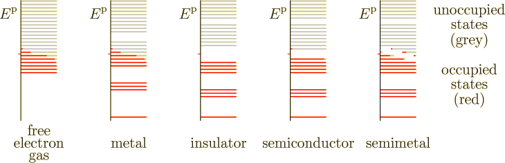
Typical energy spectra are sketched in figure 6.19. The
spectrum of a free-electron gas, noninteracting electrons in a box, is
shown to the left. The energy ![]()
 |
However, the free-electron gas assumes that there are no forces on the electrons. Inside a solid, this would only be true if the electric charges of the nuclei and fellow electrons would be homogeneously distributed throughout the entire solid. In that case the forces come equally from all directions and cancel each other out perfectly. In a true solid, forces from different directions do tend to cancel each other out, but this is far from perfect. For example, an electron very close to one particular nucleus experiences a strong attraction from that nucleus, much too strong for the rest of the solid to cancel.
The diametrical opposite of the free-electron gas picture is the case
that the atoms of the solid are spaced so far apart that they are
essentially lone atoms. In that case, of course, the
solid
would not physically be a solid at all, but a
thin gas. Lone atoms do not have a continuum of electron energy
levels, but discrete ones, as sketched to the far right in figure
6.19. One basic example is the hydrogen spectrum shown
in figure 4.8. Every lone atom in the system has the
exact same discrete energy levels. Widely spaced atoms do not conduct
electricity, assuming that not enough energy is provided to ionize
them. While for the free-electron gas conduction can be achieved by
moving a few electrons to slightly higher energy levels, for lone
atoms there are no slightly higher energy levels.
When the lone atoms are brought closer together to form a true solid, however, the discrete atomic energy levels broaden out into bands. In particular, the outer electrons start to interact strongly with surrounding atoms. The different forms that these interactions can take produce varying energies, causing initially equal electron energies to broaden into bands. The result is sketched in the middle of figure 6.19. The higher occupied energy levels spread out significantly. (The inner atomic electrons, having the most negative net energies, do not interact significantly with different atoms, and their energy levels do not broaden much. This is not just because these electrons are farther from the surrounding atoms, but also because the inner electrons have much greater kinetic and much more negative potential energy levels to start with.)
For metals, conduction now becomes possible. Electrons at the highest occupied energy level, the Fermi energy, can be moved to slightly higher energy levels to provide net motion in a particular direction. That is just like they can for a free-electron gas as discussed in the previous section. The net motion produces a current.
Insulators are different. As sketched in figure 6.19, they completely fill up the highest occupied energy band. That filled band is called the “valence band.” The next higher and empty band is called the “conduction band.”
Now it is no longer possible to prod electrons to slightly higher energy levels to create net motion. There are no slightly higher energy levels available; all levels in the valence band are already filled with electrons.
To create a state with net motion, some electrons would have to be
moved to the conduction band. But that would require large amounts of
energy. The minimum energy required is the difference between the top
of the valence band and the bottom of the conduction band. This
energy is appropriately called the “band gap” energy ![]() .
.
Resistance is determined for voltages low enough that Ohm’s law applies. Such voltages do not provide anywhere near the energy required to move electrons to the conduction band. So the electrons in an insulator are stuck. They cannot achieve net motion at all. And without net motion, there is no current. That makes the resistance infinite. In this way the band gaps are responsible for the enormous difference in resistance between metals and insulators.
Note that a normal applied voltage will not have a significant effect on the band structure. Atomic potential energies are in terms of eV or more. For the applied voltage to compete with that would require a voltage drop comparable to volts per atom. On a microscopic scale, the applied potential does not change the states.
Key Points
- Quantum mechanics allows only discrete energy levels for the electrons in a solid, and these levels group together in bands with gaps in between them.
- If the electrons fill the spectrum right up to a gap between bands, the electrons are stuck. It will require a large amount of energy to activate them to conduct electricity or heat. Such a solid is an insulator at absolute zero temperature.
- The filled band is called the valence band, and the empty band above it the conduction band.
If a material completely fills up its valence band with electrons, it is an insulator. But what materials would do that? This subsection gives a few rules of thumb.
One important rule is that the elements towards the left in the periodic table figure 5.8 are metals. A relatively small group of elements towards the right are nonmetals.
Consider first the alkali metals found in group I to the far left in
the table. The lone atoms have only one valence electron per atom.
It is in an atomic s
state that can hold two
electrons, chapter 5.9.4. Every spatial state, including
the s state, can hold two electrons that differ in spin.
Now if the lone atoms are brought closer together to form a solid, the spatial states change. Their energy levels broaden out into a band. However, the total number of states does not change. One spatial state per atom stays one spatial state per atom. Since each spatial state can hold two electrons, and there is only one, the band formed from the s states is only half filled. Therefore, like the name says, the alkali metals are metals.
In helium the spatial 1s states are completely filled with the two electrons per atom. That makes solid helium an insulator. It should be noted that helium is only a solid at very low temperatures and very high pressures. The atoms are barely held together by very weak Van der Waals forces.
The alkaline metals found in group II of the periodic table also have two valence electrons per atom. So you would expect them to be insulators too. However, like the name says, the alkaline metals are metals. What happens is that the filled band originating from the atomic s states merges with an empty band originating from the atomic p states. That produces a partially filled combined band.
This does not apply to helium because there are no 1p states. The lowest empty energy states for helium are the 2s ones. Still, computations predict that helium will turn metallic at extremely high pressures. Compressing a solid has the primary effect of increasing the kinetic energy of the electrons. Roughly speaking, the kinetic energy is inversely proportional to the square of the electron spacing, compare the Fermi energy (6.16). And increasing the kinetic energy of the electrons brings them closer to a free-electron gas.
A case resembling that of helium is ionic materials in which the ions have a noble-gas electron structure. A basic example is salt, sodium chloride. These materials are insulators, as it takes significant energy to take apart the noble-gas electron configurations. See however the discussion of ionic conductivity later in this section.
Another case that requires explanation is hydrogen. Like the alkali metals, hydrogen has only one valence electron per atom. That is not enough to fill up the energy band resulting from the atomic 1s states. So you would expect solid hydrogen to be a metal. But actually, hydrogen is an insulator. What happens is that the energy band produced by the 1s states splits into two. And the lower half is completely filled with electrons.
The reason for the splitting is that in the solid, the hydrogen atoms combine pairwise into molecules. In an hydrogen molecule, there are not two separate spatial 1s states of equal energy, chapter 5.2. Instead, there is a lowered-energy two-electron spatial state in which the two electrons are symmetrically shared. There is also a raised-energy two-electron spatial state in which the two electrons are antisymmetrically shared. So there are now two energy levels with a gap in between them. The two electrons occupy the lower-energy symmetric state with opposite spins. In the solid, the hydrogen molecules are barely held together by weak Van der Waals forces. The interactions between the molecules are small, so the two molecular energy levels broaden only slightly into two thin bands. The gap between the filled symmetric states and the empty antisymmetric ones remains.
Note that sharing electrons in pairs involves a nontrivial interaction between the two electrons in each pair. The truth must be stretched a bit to fit it within the band theory idea of noninteracting electrons. Truly noninteracting electrons would have the spatial states of the hydrogen molecular ion available to them, chapter 4.6. Here the lower energy state is one in which a single electron is symmetrically shared between the atoms. And the higher energy state is one in which a single electron is antisymmetrically shared. In the model of noninteracting electrons, both electrons occupy the lower-energy single-electron spatial state, again with opposite spins. One problem with this picture is that the single-electron states do not take into account where the other electron is. There is then a significant chance that both electrons can be found around the same atom. In the correct two-electron state, the electrons largely avoid that. Being around the same atom would increase their energy, since the electrons repel each other.
Note also that using the actual hydrogen molecular ion states may not
be the best approach. It might be better to account for the presence
of the other electron approximately using some nuclear shielding
approach like the one used for atoms in chapter 5.9. An
improved, but still approximate way of accounting for the second
electron would be to use a so-called Hartree-Fock
method. More generally, the most straightforward band theory approach
tends to work better for metals than for insulators. Alternative
numerical methods exist that work better for insulators. At the time
of writing there is no simple magic bullet that works well for every
material.
Group IV elements like diamond, silicon, and germanium pull a similar trick as hydrogen. They are insulators at absolute zero temperature. However, their 4 valence electrons per atom are not enough to fill the merged band arising from the s and p states. That band can hold 8 electrons per atom. Like hydrogen, a gap forms within the band. First the s and p states are converted into hybrids, chapter 5.11.4. Then states are created in which electrons are shared symmetrically between atoms and states in which they are shared antisymmetrically. There is an energy gap between these states. The lower energy states are filled with electrons and the higher energy states are empty, producing again an insulator. But unlike in hydrogen, each atom is now bonded to four others. That turns the entire solid into essentially one big molecule. These materials are much stronger and more stable than solid hydrogen. Like helium, hydrogen is only a solid at very low temperatures.
It may be noted that under extremely high pressures, hydrogen might become metallic. Not only that, as the smallest atom of them all, and in the absence of 1p atomic states, metallic hydrogen is likely to have some very unusual properties. It makes metallic hydrogen the holy grail of high pressure physics.
It is instructive to examine how the band theory of noninteracting
electrons accounts for the fact that hydrogen is an insulator. Unlike
the discussion above, band theory does not actually look at the number
of valence electrons per atom. For one, a solid may consist of
atoms of more than one kind. In general, crystalline solids consist
of elementary building blocks called primitive cells
that can involve several atoms. Band theory predicts the solid to be
a metal if the number of electrons per primitive cell is odd.
If the number of electrons per primitive cell is even, the material
may be an insulator. In solid hydrogen each primitive cell holds a
complete molecule, so there are two atoms per primitive cell. Each
atom contributes an electron, so the number of electrons per primitive
cell is even. According to band theory, that allows hydrogen to be an
insulator. In a similar way group V elements can fill up their
valence bands with an odd number of valence electrons per atom. And
like hydrogen, diamond, silicon, and germanium have two atoms per
primitive cell, reflecting the gap that forms in the merged s and p
bands.
Of course, that cannot be the complete story. It does not explain why
atoms towards the right in the periodic table would group together
into primitive cells that allow them to be insulators. Why don't the
atoms to the left in the periodic table do the same? Why don't the
alkali metals group together in two-atom molecules like hydrogen does?
Qualitatively speaking, metals are characterized by valence electrons
that are relatively loosely bound. Suppose you compare the size of
the 2s state of a lithium atom with the spacing of the atoms in solid
lithium. If you do, you find that on average the 2s valence electron
is no closer to the atom to which it supposedly
belongs
than to the neighboring atoms. Therefore, the
electrons are what is called delocalized.
They are not
bound to one specific location in the atomic crystal structure. So
they are not really interested in helping bond their
particular atom to its immediate neighbors. On the other hand, to the
right in the periodic table, including hydrogen and helium, the
valence electrons are much more tightly held. To delocalize them
would require that the atoms would be squeezed much more tightly
together. That does not happen under normal pressures because it
produces very high kinetic energy of the electrons.
Where hydrogen refuses to be a metal with one valence electron per atom, boron refuses to do so with three. However, boron is very ambivalent about it. It does not really feel comfortable with either metallic or covalent behavior. A bit of impurity can readily turn it metallic. That great sensitivity to impurity makes the element very hard to study. At the time of writing, it is believed that boron has a covalent ground state under normal pressures. The convoluted crystal structure is believed to have a unit cell with either 12 or 106 atoms, depending on precise conditions.
In group IV, tin is metallic above 13 ![]() C
C
It should further be noted that band theory can be in error because it ignores the interactions between the electrons. “Mott insulators” and “charge transfer insulators” are, as the name says, insulators even though conventional band theory would predict that they are metals.
Key Points
- In the periodic table, the group I, II, and III elements are normally metals.
- Hydrogen and helium are nonmetals. Don’t ask about boron.
- The group IV elements diamond, silicon, and germanium are insulators at absolute zero temperature.
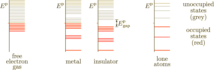
Temperature can have significant effects on electrical conduction. As the previous section noted, higher temperature decreases the conduction in metals, as there are more crystal vibrations that the moving electrons can get scattered by. But a higher temperature also changes which energy states the electrons occupy. And that can produce semiconductors.
Figure 6.19 showed which energy states the electrons
occupy at absolute zero temperature. There are no electrons with
energies above the Fermi level indicated by the red tick mark. Figure
6.20 shows how that changes for a nonzero temperature.
Now random thermal motion allows electrons to reach energy levels up
to roughly ![]()
![]()
![]()
It does not make much difference for a free-electron gas or a metal.
However, for an insulator it may make a dramatic difference. If the
band gap is not too large compared to ![]() ,
,
It is often more convenient to think of the moving holes instead of the electrons as the electric current carriers in the valence band. Since a hole means that a negatively charged electron is missing, a hole acts much like a positively charged particle would.
Because both the electrons in the conduction band and the holes in the valence band allow some electrical conduction, the original insulator has turned into what is called a “semiconductor.”
The previous section mentioned that a classical picture of moving electrons simply does not work for metals. Their motion is much too much restrained by a lack of available empty energy states. However, the conduction band of semi-conductors is largely empty. Therefore a classical picture works much better for the motion of the electrons in the conduction band of a semiconductor.
Key Points
- For semiconductors, conduction can occur because some electrons from the valence band are thermally excited to the conduction band.
- Both the electrons that get into the conduction band and the holes they leave behind in the valence band can conduct electricity.
One additional type of electron energy spectrum for solids should be mentioned. For a “semimetal,” two distinct energy bands overlap slightly at the Fermi level. In terms of the simplistic spectra of figure 6.19, that would mean that semimetals are metals. Indeed they do allow conduction at absolute zero temperature. However, their further behavior is noticeably different from true metals because the overlap of the two bands is only small. One difference is that the electrical conduction of semimetals increases with temperature, unlike that of metals. Like for semiconductors, for semimetals a higher temperature means that there are more electrons in the upper band and more holes in the lower band. That effect is sketched to the far right in figure 6.20.
The classical semimetals are arsenic, antimony, and bismuth. Arsenic
and antimony are not just semimetals, but also
metalloids,
a group of elements whose chemical
properties are considered to be intermediate between metals and
nonmetals. But semimetal and metalloid are not the same thing.
Semimetals do not have to consist of a single element. Conversely,
metalloids include the semiconductors silicon and germanium.
A semimetal that is receiving considerable attention at the time of writing is graphite. Graphite consists of sheets of carbon atoms. A single sheet of carbon, called graphene, is right on the boundary between semimetal and semiconductor. A carbon nanotube can be thought of as a strip cut from a graphene sheet that then has its long edges attached together to produce a cylinder. Carbon nanotubes have electrical properties that are fundamentally different depending on the direction in which the strip is cut from the sheet. They can either be metallic or nonmetallic.
Key Points
- Semimetals have properties intermediate between metals and semiconductors.
The valence electrons in metals are not just very good conductors of electricity, but also of heat. In insulators electrons do not assist in heat conduction; it takes too much energy to excite them. However, atomic vibrations in solids can conduct heat too. For example, diamond, an excellent electrical insulator, is also an excellent conductor of heat. Therefore the differences in heat conduction between solids are not by far as large as those in electrical conduction. Because atoms can conduct significant heat, no solid material will be a truly superb thermal insulator. Practical thermal insulators are highly porous materials whose volume consists largely of voids.
Key Points
- Electrons conduct heat very well, but atoms can do it too.
- Practical thermal insulators use voids to reduce atomic heat conduction.
It should be mentioned that electrons do not have an absolute monopoly
on electrical conduction in solids. A different type of electrical
conduction is possible in ionic solids. These solids consist of a
mixture of positively and negatively charged ions. Positive ions, or
cations,
are atoms that have lost one or more
electrons. Negative ions, or anions,
are atoms that
have absorbed one or more additional electrons. A simple example of a
ionic solid is salt, which consists of ![]()
![]()
Typical defects include vacancies,
in which an atom is
missing from the crystal structure, and interstitials,
in which an additional atom has been forced into one of the small gaps
between the atoms in the crystal. Now if a ion gets removed from its
normal position in the crystal to create a vacancy, it must go
somewhere. One possibility is that it gets squeezed in between the
other atoms in the crystal. In that case both a vacancy and an
interstitial have been produced at the same time. Such a combination
of a vacancy and an interstitial is called a “Frenkel defect.” Another possibility occurs in, for example,
salt; along with the original vacancy, a vacancy for a ion of the
opposite kind is created. Such a combination of two opposite
vacancies is called a “Schottky defect.” In this case there is no need to squeeze an
atom in the gaps in the crystal structure; there are now equal numbers
of ions of each kind to fill the surrounding normal crystal sites.
Creating defects in Frenkel or Schottky pairs ensures that the
complete crystal remains electrically neutral as it should.
Impurities are another important defect. For example, in salt a
![]()
![]()
![]() ,
,![]()
![]()
For salt, the main conduction mechanism is by natrium vacancies. But the ionic conductivity of salt is almost immeasurably small at room temperature. That is due to the high energy needed to create Schottky defects and for natrium ions to migrate into the natrium vacancies. Indeed, whatever little conduction there is at room temperature is due to impurities. Heating will help, as it increases the thermal energy available for both defect creation and ion mobility. As seen from the Maxwell-Boltzmann distribution discussed earlier, thermal effects increase exponentially with temperature. Still, even at the melting point of salt its conductivity is eight orders of magnitude less than that of metals.
There are however ionic materials that have much higher
conductivities. They cannot compete with metals, but some ionic
solids can compete with liquid electrolytes. These solids may be
referred to as “solid electrolytes, “fast ion conductors,” or “superionic conductors.” They are important for such
applications as batteries, fuel cells, and gas sensors.
Yttria-stabilized zirconia is an example, although unfortunately only
at temperatures around 1 000 ![]() C
C![]()
Crystal surfaces are also crystal defects, in a sense. They can enhance ionic conductivity. For example, nanoionics can greatly improve the ionic conductivity of poor ionic conductors by combining them in nanoscale layers.
Key Points
- In ionic solids, some electrical conduction may occur through the motion of the ions instead of individual electrons.
- It is important for applications such as batteries, fuel cells, and gas sensors.