|
|
|
|
|
Next: 7. Time Evolution |
|
Thermoelectric effects can be used to make solid-state refrigeration devices, or to sense temperature differences, or to convert thermal energy directly into electricity. This section explains the underlying principles.
There are three different thermoelectric effects. They are named the Peltier, Seebeck, and Thomson effects after the researchers who first observed them. Thomson is better known as Kelvin.
These effects are not at all specific to semiconductors. However semiconductors are particularly suitable for thermoelectric applications. The reason is that the nature of the current carriers in semiconductors can be manipulated. That is done by doping the material as described in section 6.23. In an n-type doped semiconductor, currents are carried by mobile electrons. In a p-type doped semiconductor, the currents are carried by mobile holes, quantum states from which electrons are missing. Electrons are negatively charged particles, but holes act as positively charged ones. That is because a negatively charged electron is missing from a hole.
Thermoelectric cooling can be achieved through what is called the
Peltier effect.
The top part of figure 6.37
shows a schematic of a Peltier cooler. The typical device consists of
blocks of a semiconductor like bismuth telluride that are alternately
doped n-type and p-type. The blocks are electrically
connected by strips of a metal like copper.
The connections are made such that when a current is passed through the device, both the n-type electrons and the p-type holes move towards the same side of the device. For example, in figure 6.37 both electrons and holes move to the top of the device. The current however is upward in the p-type blocks and downward in the n-type blocks. (Since electrons are negatively charged, their current is in the direction opposite to their motion.) The same current that enters a metal strip from one block leaves the strip again through the other block.
![\begin{figure}\centering
\setlength{\unitlength}{1pt}
\begin{picture}(405,19...
...kebox(0,0)[lt]{A}}
\put(8,46){\makebox(0,0)[lt]{B}}
\end{picture}
\end{figure}](img1507.gif) |
Consider now a metal strip at the top of the device in figure 6.37. Such a strip needs to take in a stream of conduction-band electrons from an n-type semiconductor block A. It must drop the same number of electrons into the valence-band holes coming in from a p-type semiconductor block B to eliminate them. As illustrated by the top arrow between the spectra at the bottom of figure 6.37, this lowers the energy of the electrons. Therefore energy is released, and the top strips get hot.
However, a bottom strip needs to take electrons out of the valence band of a p-type semiconductor B to create the outgoing holes. It needs to put these electrons into the conduction band of an n-type semiconductor A. That requires energy, so the bottom strips lose energy and cool down. You might think of it as evaporative cooling: the bottom strips have to give up their electrons with the highest thermal energy.
The net effect is that the Peltier cooler acts as a heat pump that removes heat from the cold side and adds it to the hot side. It can therefore provide refrigeration at the cold side. At the time of writing, Peltier coolers use a lot more power to operate than a refrigerant-based device of the same cooling capability. However, the device is much simpler, and is therefore more suitable for various small applications. And it can easily regulate temperatures; a simple reversal of the current turns the cold side into the hot side.
Note that while the Peltier device connects p and n type semiconductors, it does not act as a diode. In particular, even in the bottom strips there is no need to raise electrons over the band gap of the semiconductor to create the new electrons and holes. Copper does not have a band gap.
It is true that the bottom strips must take electrons out of the p-type valence band and put them into the n-type conduction band. However, as the spectra at the bottom of figure 6.37 show, the energy needed to do so is much less than the band gap. The reason is that the p-type spectrum is raised relative to the n-type one. That is an effect of the electrostatic potential energies that are different in the two semiconductors. Even in thermal equilibrium, the spectra are at unequal levels. In particular, in equilibrium the electrostatic potentials adjust so that the chemical potentials, shown as red tick marks in the spectra, line up. The applied external voltage then decreases the energy difference even more.
The analysis of Peltier cooling can be phrased more generally in terms
of properties of the materials involved. The “Peltier coefficient” ![]()
Now consider the energy balance of a top strip in figure
6.37. An electric current ![]()
![]()
![]()
![]()
![]()
![]()
![]()
For the top strips in figure 6.37, ![]()
![]()
![]()
If there is a temperature gradient in the semiconductors in addition to the current, and there will be, it too will create a heat flow, {A.11}. This heat flow can be found using what is known as Fourier’s law. It is bad news as it removes heat from the hot side and conducts it to the cold side.
A more quantitative understanding of the Peltier effect can be obtained
using some ballpark Peltier coefficients. Consider again the spectra
in figure 6.37. In the n-type semiconductor, each
conduction electron has an energy per unit charge of about
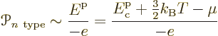
The reason for doing the latter has to do with the fact that in thermal equilibrium, all solids in contact have the same chemical potential. That makes the chemical potential a convenient reference level of energy. The idea can be described graphically in terms of the spectra of figure 6.37. In the spectra, the chemical potential is indicated by the red tick marks on the vertical axes. Now consider again the energy change in transferring electrons between the n- and p-type materials. What determines it is how much the n-type electrons are higher in energy than the chemical potential and how much electrons put in the p-type holes are lower than it. (This assumes that the current remains small enough that the chemical potentials in the two semiconductors stay level. Otherwise theoretical description would become much more difficult.)
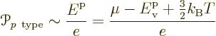
As this picture suggests, for the holes in the p-type
semiconductor, the energy should be taken to be increasing downwards
in the electron spectrum. It takes more energy to create a hole by
taking an electron up to the Fermi level if the hole is lower in the
spectrum. Therefore the Peltier coefficient of the p-doped
semiconductor is
Note that both formulae are just ballparks. The thermal energy
dragged along by a current is not simply the thermal equilibrium
distribution of electron energy. The average thermal kinetic energy
per current carrier to be used turns out to differ somewhat from
![]() .
.
It is however interesting to compare the above semiconductor ballparks
to one for metals:
The ballpark above implies that the Peltier coefficient of a metal is very much less than that of a doped semiconductor. It should however be noted that while the ballpark does give the rough order of magnitude of the Peltier coefficients of metals, they tend to be noticeably larger. Worse, there are quite a few metals whose Peltier coefficient is positive, unlike the ballpark above says.
To some extent, the lower Peltier coefficients of metals are
compensated for by their larger electrical conductivity. A
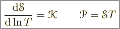
nondimensional figure of merit can be defined for thermoelectric
materials as, {A.11}:
Key Points
- In the Peltier effect, a current produces cooling or heating when it passes through the contact area between two solids.
- The heat released is proportional to the current and the difference in Peltier coefficients of the materials.
- Connections between oppositely-doped semiconductors work well.
Thermoelectric temperature sensing and power generation can be
achieved by what is known as the Seebeck effect.
It is
in some sense the opposite of the Peltier effect of the previous
subsection.
Consider the configuration shown in figure 6.38. Blocks of n-type and p-type doped semiconductors are electrically connected at their tops using a copper strip. Copper strips are also attached to the bottoms of the semiconductor blocks. Unlike for the Peltier device, no external voltage source is attached. In the pure Seebeck effect, the bottom strips are electrically not in contact at all. So there is no current through the device. It is what is called an open-circuit configuration.
To achieve the Seebeck effect, heat from an external heat source is added to the top copper strip. That heats it up. Heat is allowed to escape from the bottom strips to, say, cooling water. This heat flow pattern is the exact opposite of the one for the Peltier cooler. If heat went out of the strips of your Peltier cooler at the cold side, it would melt your ice cubes.
But the Peltier cooler requires an external voltage to be supplied to keep the device running. The opposite happens for the Seebeck generator of figure 6.38. The device itself turns into a electric power supply. A voltage difference develops spontaneously between the bottom two strips.
That voltage difference can be used to determine the temperature of the top copper strip, assuming that the bottom strips are kept at a known temperature. A device that measures temperatures this way is called a “thermocouple.”
Alternatively, you can extract electrical power from the voltage difference between the two bottom terminals. In that case the Seebeck device acts as a “thermoelectric generator.” Of course, to extract power you need to allow some current to flow. That will reduce the voltage below the pure Seebeck value.
To describe why the device works physically is not that easy. To understand the basic idea, consider an arbitrary point P in the n-type semiconductor, as indicated in figure 6.38. Imagine yourself standing at this point, shrunk down to microscopic dimensions. Due to random heat motion, conduction electrons come at you randomly from both above and below. However, those coming from above are hotter and so they come towards you at a higher speed. Therefore, assuming that all else is the same, there is a net electron current downwards at your location. Of course, that cannot go on, because it moves negative charge down, charging the lower part of the device negative and the top positive. This will create an electric field that slows down the hot electrons going down and speeds up the cold electrons going up. The voltage gradient associated with this electric field is the Seebeck effect, {A.11}.
In the Seebeck effect, an incremental temperature change ![]()
![]()
This coefficient is sometimes called the “Seebeck coefficient.” However, it is usually called the
thermopower” or “thermoelectric power.
These names are much better, because the Seebeck coefficient describes
an open-circuit voltage, in which no power is produced. It has units
of V/K. It is hilarious to watch the confused faces of those hated
nonspecialists when a physicist with a straight face describes
something that is not, and cannot be, a power as the
thermopower.
The net voltage produced is the integrated total voltage change over
the lengths of the two materials. If ![]()
![]()
The above equation assumes that the copper strips conduct heat well enough that their temperature is constant, (or alternatively, that materials A and B are in direct contact with each other at their top edges and with the voltmeter at their bottom edges). Otherwise you would need to add an integral over the copper.
Note from the above equation that, given the temperature ![]()
![]()
![]()
![]() .
.
![\begin{figure}\centering
\setlength{\unitlength}{1pt}
\begin{picture}(400,14...
...le{32}}
\put(0,-36){\makebox(0,0)[b]{\scriptsize0}}
\end{picture}
\end{figure}](img1535.gif) |
It is sometimes suggested, even by some that surely know better like [22, p. 14-9], that the Seebeck potential is due to jumps in potential at the contact surfaces. To explain the idea, consider figure 6.39. In this figure materials A and B have been connected directly in order to simplify the ideas. It turns out that the mean electrostatic potential inside material A immediately before the contact surface with material B is different from the mean electrostatic potential inside material B immediately after the contact surface. The difference is called the Galvani potential. It is due to the charge double layer that exists at the contact surface between different solids. This charge layer develops to ensure that the chemical potentials are the same at both sides of the contact surface. Equality of chemical potentials across contact surfaces is a requirement for thermal equilibrium. Electrostatic potentials can be different.
If you try to measure this Galvani potential directly, like with the bottom voltmeter in figure 6.39, you fail. The reason is that there are also Galvani potential jumps between materials A and B and the leads of your voltmeter. Assume for simplicity that the leads of your voltmeter are both made of copper. Because the chemical potentials are pairwise equal across the contact surfaces, all four chemical potentials are the same, including the two in the voltmeter leads. Therefore, the actual voltmeter can detect no difference between its two leads and gives a zero reading.
Now consider the top voltmeter in figure 6.39. This
voltmeter does measure a voltage. Also in this case, the contact
surfaces between the leads of the voltmeter and materials A and B are
at a different temperature ![]()
![]()
It may be neat, but unfortunately it is also all wrong. The fact that the dependence on the temperature distribution drops out of the final result is just a mathematical coincidence. As long as the changes in intrinsic chemical potential can be ignored, the Galvani potential jumps still sum to zero. Not to the measured potential. After all, in that case the voltage changes over the lengths of the materials are the same as the chemical potential changes. And because they already sum to the measured voltage, there is nothing left for the Galvani jumps. Consider for example the free-electron gas model of metals. While its intrinsic chemical potential does change with temperature, {D.62}, that change is only one third of the potential change produced by the Seebeck coefficient given in addendum {A.11}. Galvani potential changes then sum to only a third of the measured potential. No, there is no partial credit.
It should also be pointed out that the Seebeck effect of a material is not directly measurable. Figure 6.40 illustrates an attempt to directly measure the Seebeck effect of material A. Unfortunately, the only thing that changes compared to figure 6.39 is that the two leads of the voltmeter take over the place of material B. Unless the two leads are attached to points of equal temperature, they are an active part of the total Seebeck effect measured. (Superconductors should have their Seebeck coefficient zero. However, finding superconductors that still are superconductors if they are in thermal contact with real-life temperatures is an obvious issue.)
Kelvin discovered that you can find the Seebeck coefficient
![]()
![]()
You might wonder where the charges that transfer between the hot and cold sides in the Seebeck effect end up. In thermal equilibrium, the interiors of solids need to stay free of net electric charge, or a current would develop to eliminated the charge difference. But in the Seebeck effect, the solids are not in thermal equilibrium. It is therefore somewhat surprising that the interiors do remain free of net charge. At least, they do if the temperature variations are small enough, {A.11}. So the charges that transfer between hot and cold, and so give rise to the Seebeck potential difference, end up at the surfaces of the solids. Not in the interior. Even in the Seebeck effect.
Key Points
- The Seebeck effect produces a usable voltage from temperature differences.
- It requires two different materials in electrical contact to span the temperature difference.
- The voltage is the difference in the integrals of the Seebeck coefficients of the two materials with respect to temperature.
- The Seebeck coefficient is usually called thermopower because it is not power.
The Thomson effect,” or “Kelvin heat,
describes the heat release in a material with a current through it.
This heat release is directly measurable. That is unlike the Peltier
and Seebeck effects, for which only the net effect of two different
materials can be measured. Since the Peltier and Seebeck coefficients
can be computed from the Thomson one, in principle the Thomson effect
allows all three thermoelectric coefficients to be found without
involving a second material.
Thomson, who later became lord Kelvin, showed that the net energy
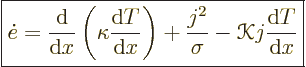
accumulation per unit volume in a bar of material with a current
through it can be written as:
Kelvin effectis not used because it is already in common use for something else.) The coefficient
It may be noted that for devices in which the Thomson effect is important, the figure of merit introduced earlier becomes less meaningful. In such cases, a second nondimensional number based on the Kelvin coefficient will also affect device performance.
The other two thermoelectric coefficients can be computed from the
Kelvin one using the Kelvin, or Thomson, relationships
{A.11}:
That requires of course that you find the Kelvin coefficient over the complete temperature range. But you only need to do it for one material. As soon as you accurately know the thermoelectric coefficients for one material, you can use that as the reference material to find Peltier and Seebeck coefficients for every other material. Lead is typically used as the reference material, as it has relatively low thermoelectric coefficients.
Of course, if it turns out that the data on your reference material are not as accurate as you thought they were, it would be very bad news. It will affect the accuracy of the thermoelectric coefficients of every other material that you found using this reference material. A prediction on whether such a thing was likely to happen for lead could be derived from what is known as Murphy’s law.
Key Points
- The Thomson effect, or Kelvin heat, describes the internal heating in a material with a current going through it. More precisely, it describes the part of this heating that is due to interaction of the current with the temperature changes.
- Unlike the Peltier and Seebeck coefficients, the Kelvin (Thomson) coefficient can be measured without involving a second material.
- The Kelvin (Thomson) relations allow you to compute the Peltier and Seebeck coefficients from the Kelvin one.

![\begin{figure}\centering
\setlength{\unitlength}{1pt}
\begin{picture}(405,18...
...b]
{$\circ$\ \ hole (\emph{p}-type semiconductor)}}
\end{picture}
\end{figure}](img1524.gif)
![\begin{figure}\centering
\setlength{\unitlength}{1pt}
\begin{picture}(400,94...
...{32}}
\put(-25,-36){\makebox(0,0)[b]{\scriptsize0}}
\end{picture}
\end{figure}](img1536.gif)